
Microvias in Flex Circuit
With modern electronics becoming increasingly more compact, it is essential for PCBs to pack as much functionality as possible into a small space. One way to do this is by using various via construction techniques. Understanding the role of microvias in flex circuit can help you make informed decisions about design and fabrication.
A microvia is a blind hole in a printed circuit board (PCB) that connects layers of the same conductor pattern by allowing copper to flow through it from one layer to the other. They are drilled at a 1:1 aspect ratio or smaller and are plated with copper to establish the electrical connection between the layers. The process of drilling microvias involves using a laser to etch the desired location on the circuit board’s dielectric layer, then filling it with copper through electroless or electrolytic deposition. The microvias are then subject to a desmearing step to ensure that there are no residual materials left behind and that the plated copper has uniform micro coverage on all the via walls.
When designing a PCB with microvias, it is critical to follow the IPC’s guidelines when selecting the size of each individual hole. It is recommended to stay below a 4:1 aspect ratio, since anything larger will be difficult to plate with a reliable process. This will also ensure that the via is adequately sized for the signal to pass through it without interference or distortion.
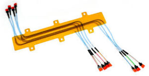
The Role of Microvias in Flex Circuit
As the industry continues to shrink device form factors, it is often necessary to place more SMT components in a flex or rigid-flex circuit. This can be a challenge because standard through-holes may not fit inside the pads for tight pitch BGAs and other SMT devices on flex or rigid-flex boards.
To overcome this challenge, the use of HDI technology and staggered or stacked microvias is often used on flex and flex circuit with SMT components. This construction technique is especially useful for reducing cost when creating high-speed circuits, as it provides for lower trace lengths.
In addition, the smaller microvia holes require fewer layers to pass through them, which can help reduce overall manufacturing costs for a circuit board. Additionally, the use of laser-drilled microvias can result in a more stable and durable final product.
Staggered or stacked microvias can be fabricated on either single-sided or double-access flex circuits. Single-sided flex circuits have a single conductor layer on a flexible dielectric film and feature component termination features that are accessible only from one side. Double access flex circuits, on the other hand, have two conductor layers with access to selected features on both sides of the board. However, in both types of flex circuits, it is important to avoid stacking microvias more than two high. Recent industry experience suggests that this can cause a large number of thermal cycles to the microvias, which can result in failure. This is due to the mismatch between copper and dielectric material CTEs.