
printed circuit board design
Conducting a thorough printed circuit board (PCB) design review is a critical step in the development process to ensure the quality, functionality, and reliability of the final product. A comprehensive design review involves a systematic evaluation of various aspects of the PCB layout, schematics, and design documentation by a team of experts, including designers, engineers, and stakeholders. To conduct a thorough PCB design review, several key steps and considerations must be taken into account.
Firstly, it is essential to establish clear objectives and criteria for the design review. Define the goals, scope, and expectations of the review, including specific areas to be evaluated, such as signal integrity, component placement, routing, manufacturability, and compliance with standards and requirements. Establishing clear criteria helps ensure that the review is focused and productive, enabling reviewers to identify potential issues and assess design performance effectively.
Next, assemble a diverse team of reviewers with expertise in relevant areas of printed circuit board design, including electrical engineering, mechanical engineering, manufacturing, quality assurance, and regulatory compliance. Involve stakeholders from different departments and disciplines to provide diverse perspectives and insights during the review process. Ensure that all team members are familiar with the design objectives, requirements, and expectations to facilitate meaningful discussions and feedback.
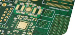
how do you conduct a thorough printed circuit board design review?
Before the review session, distribute the PCB layout, schematics, design documentation, and any relevant specifications or standards to all reviewers. Encourage reviewers to familiarize themselves with the design materials and prepare questions, comments, and observations in advance. Providing adequate time for reviewers to review the documentation independently helps ensure that the review session is productive and focused on addressing specific issues and concerns.
During the review session, systematically evaluate the PCB design according to the established objectives and criteria. Start by reviewing the schematics to verify the correctness of the circuit connections, component values, and functional requirements. Evaluate the PCB layout to assess component placement, routing topology, signal integrity, power distribution, and thermal management. Use design review checklists or guidelines to ensure that all relevant aspects of the design are examined thoroughly.
Encourage active participation and open communication among team members during the review session. Foster a collaborative environment where reviewers can ask questions, share insights, and provide constructive feedback on the design. Discuss any identified issues, trade-offs, and potential solutions to address design challenges effectively. Document all feedback, comments, and action items raised during the review session for follow-up and resolution.
After the review session, compile a summary report documenting the findings, conclusions, and recommendations from the review. Include a list of identified issues, proposed solutions, and action items to be addressed by the design team. Distribute the review report to all stakeholders and follow up on action items to ensure that any identified issues are resolved promptly and effectively.
Finally, conduct follow-up reviews as needed to verify that the recommended changes have been implemented and to assess the impact on the design. Monitor the progress of the design iteration and incorporate any lessons learned from the review process into future design iterations. By conducting thorough and systematic design reviews throughout the development process, designers can identify and address potential issues early, optimize design performance, and ensure the successful realization of high-quality, reliable PCB designs.